PCB Layout
1.Product and service Introduction of PCB Layout
With our PCB design team, PCB manufacturing team, PCBA factory team and component procurement team, EDADOC is committed to providing customized, R&D proofing and flexible solutions for small and medium-sized batch PCB design and manufacturing. In 20 years, EDADOC has formed a one-stop hardware innovation platform where we turn our customers schematic diagrams into prototypes and fully-formed products.
2.Product Parameter (Specification) of PCB Layout
Maximum design floors 56th floor | Minimum via 6mil (4mil laser hole) | Maximum number of PINs 150000+ | Maximum number of BGAs 120+ |
Maximum connection 120+ | Minimum BGA PIN spacing 0.3mm | Minimum line weight 2.4mil | Highest speed signal 112G-PAM4 |
3.Product Feature And Application of PCB Layout
Communications Equipment
switch, router, various 3G/4G/5G office/terminal equipment, backbone and access network transmission equipment, optical network, network transmission storage equipment, mass storage, etc
Computer Electronics
servers, notebooks, network storage, tablets, hyperbooks, cloud computing, etc
Semiconductor
integrated circuit, consumer electronics, communication system, photovoltaic power generation, lighting, high-power power conversion and other chips
Consumer Electronics
smart phones, PDAs, digital cameras, e-books, GPS, wearable devices, VR, intelligent Internet of Things, etc
Medical Devices
ultrasound, nuclear magnetic resonance equipment, CT, IVD in vitro diagnosis, infrared temperature measurement, blood coagulation detection, nucleic acid analyzer, digital X-ray imaging, dry chemical analyzer, chemiluminescence instrument and other detection, analysis and monitoring equipment
Industrial Control Systems
artificial intelligence, machine vision, intelligent manufacturing equipment, smart grid, distribution network equipment, clean energy equipment, engineering machinery, agricultural machinery, fire fighting equipment and other industrial automation equipment
Rail Transportation
new energy vehicles, auto drive system, automobile intelligent network management system, rail transit vehicles and various electromechanical equipment, rail transit autonomous operation system, train dispatching command system, testing equipment, etc
4.Product Details of PCB Layout
PCB Design Company with Over 700 Engineers
More than 10 PCB design service networks nationwide
Effective training program that encourages strong communication
Early cooperation with chip companies and progressive approach to technology
“Standing on the shoulders of giants,” is our belief and approach to gaining expertise
Cutting-edge technology from Silicon Valley
More Than 20 Years of Industry Experience
Over 10,000 PCB design projects every year
Held over 100 technical training seminars
Countless customers gained by word of mouth
Stellar project and consulting experience
SI, PI, EMC, PCB, DFM specialization
Quality Above All Else
Quality: provide design services according to customers’ specifications; first-class training program
Self-Inspection: layout, wiring, high-speed, thermal design, structure, etc.; Follow the check list of our strict quality control system
Review: The senior expert team participates in the review and comprehensively checks the principal design, DFM, DFT, EMC, thermal design, etc.
Mutual Inspection: execute standardized and strictly controlled mutual inspection system; complete DFM review process
Shorten Design Delivery Time by 30-50% To Meet Our Customers’ Needs
Large Team of 700+ PCB engineers
Reuse Designs: reuse mature module rules to shorten delivery time
Global Outlets: convenient communication with local teams
Senior Team: professional team with senior engineers
Concurrent Design: can provide 7x24 parallel services for multiple people
Each engineer has experience in designing hundreds of PCBs
5.Product Qualification of PCB Layout
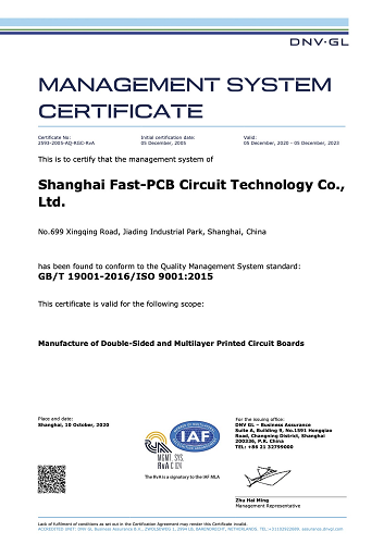
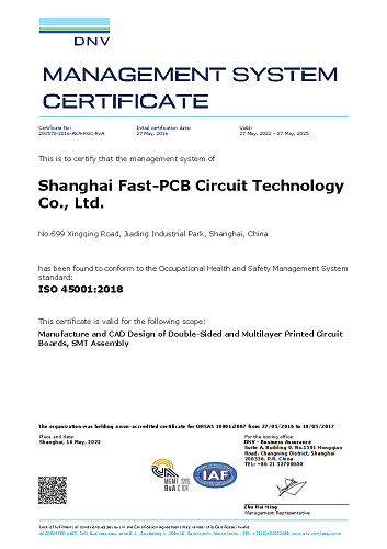
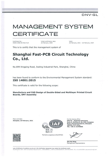
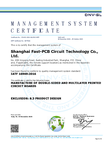
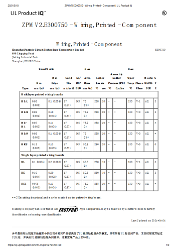
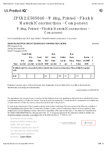
Fast-PCB is certified by ISO 9001:2015, ISO 14001:2015, ISO 45001:2018,IATF 16949:2016 and registered with US and Canada UL,
E300750 - Wiring, Printed - Rigid
E505046 - Wiring, Printed - Flexible
6.Deliver,Shipping And Serving of PCB Layout
We can dispatch goods via different express companies, like DHL, UPS, TNT and FedEx.
If the customer has dedicated forwarder, we can support ex-works delivery term as well.
7.Company Introduction
Fast PCB is located in the Jiading Industrial Zone of Shanghai. Since its establishment in April 2004, it has been committed to the production, manufacturing, and research and development services of high-precision, medium and small batch, and fast printed circuit boards, providing professional, reliable, efficient, and high-quality services for domestic and foreign high-tech enterprises and research institutions. The company covers an area of 28000 square meters, with a factory area of approximately 27000 square meters.
The company team has industry-leading experience in small and medium-sized batch and sample manufacturing of printed circuit boards, quickly providing high-quality high-tech products, widely used in various fields such as communication, industrial control, computer applications, aerospace, medical, automotive, testing instruments, etc. Our expertise lies in the management of multiple varieties, small and medium-sized batch rapid production models.