PCB Laser Drilling
1.Product and service Introduction of PCB Laser Drilling
High Density Interconnect PCB. HDI has small size, high circuit distribution density, and good transmission efficiency, conducive to the use of advanced packaging technology, the cost is lower than traditional PCB when the layers exceeds 8L, we have very good cooperation relationship with almost the popular express companies like DHL, UPS, TNT and FedEx.
2.Product Parameter (Specification) of PCB Laser Drilling
Layer Count: 40 Max. | Material: Mid and high Tg, High Speed or high frequency, Resistance/Capacitance embedded, etc. | MicroVia: 0.075um min. | Surface Treatment: HASL, HASL Lead Free, ENIG, ENEPIG, IAg, ISn, Flash Gold, Gold Plating, OSP, etc |
Solder Mask: Green White Black Yellow Blue Red Etc. | Silkscreen: Green White Black Yellow Gray Etc. | Line/Space: 0.075/0.075 um min. | Reliability: 100% Electrical Test 4-wire Test Impedance Test RoHS Test Thermal Stress Test High Voltage Insulation Resistance Test Ionic Contamination Test Solderability Test Microsection Analysis Insulation Resiatance Test Peel-off Strength Test Dielectric Loss Test Etc. |
3.Product Feature And Application of PCB Laser Drilling
01 Small, high-density circuit distribution and high transmission efficiency.
02 The design of blind holes and buried holes makes the product occupy a small space, which is in line with the trend of light, thin, miniaturized of mobile electronic equipment.
03 Variety of stacks, diverse selection of raw materials, development towards high-end multilayer and Anylayer.
4.Product Details of PCB Laser Drilling
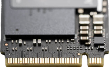
Fast-PCB can fabricate diverse HDI PCB prototypes, which has fine line and narrow space designed, we could follow class 3 of IPC 6016.
5.Product Qualification of PCB Laser Drilling
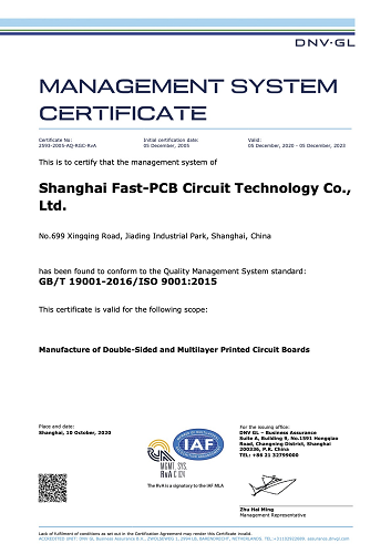
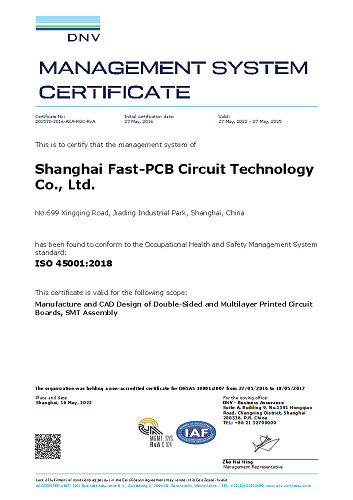
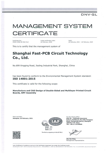
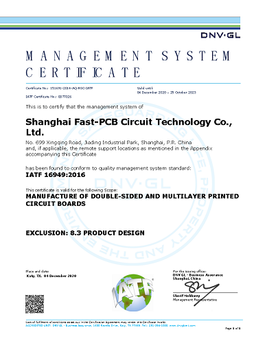
Fast-PCB is certified by ISO 9001:2015, ISO 14001:2015, ISO 45001:2018,
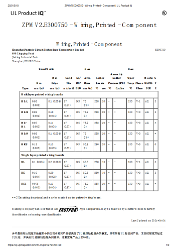
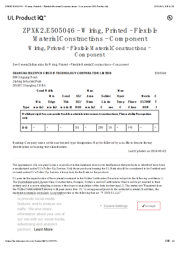
IATF 16949:2016 and registered with US and Canada UL,
E300750 - Wiring, Printed - Rigid
E505046 - Wiring, Printed - Flexible
6.Deliver,Shipping And Serving of PCB Laser Drilling
We can dispatch goods via different express companies, like DHL, UPS, TNT and FedEx.
If the customer has dedicated forwarder, we can support ex-works delivery term as well.
7.Company Introduction
Fast PCB is located in the Jiading Industrial Zone of Shanghai. Since its establishment in April 2004, it has been committed to the production, manufacturing, and research and development services of high-precision, medium and small batch, and fast printed circuit boards, providing professional, reliable, efficient, and high-quality services for domestic and foreign high-tech enterprises and research institutions. The company covers an area of 28000 square meters, with a factory area of approximately 27000 square meters.
The company team has industry-leading experience in small and medium-sized batch and sample manufacturing of printed circuit boards, quickly providing high-quality high-tech products, widely used in various fields such as communication, industrial control, computer applications, aerospace, medical, automotive, testing instruments, etc. Our expertise lies in the management of multiple varieties, small and medium-sized batch rapid production models.